I’d like to build one but not with the round pcb . Im having difficulty viewing them if their is. I can seem to bring up the gerber files in Dip Trace which is what I usually draw the import to copper cam which generate the G code for a 3 axis pcb mill… If i could bring up the copper template I could just give it a reticular footprint then I cand creat and external case and heatsink.
Im having difficulty doing that and dont know why. As a stand alone application eagle starts but then never opens. It opens in fusion 360 3d modeling but I haven’t been able to import the gerbers to it or copper cam to cut a board on my pcb mill. I cant see the full schematic of the Komar whic is what Im after. . The pcb tenmplate would be nice also.
I draw in dip trace and my milling application is copper cam.
I exported the schematic to PDF for you: Komar.pdf (153.7 KB)
I am not sure how to help with your Eagle issues. If you’re on GNU/Linux, inspect the stderr output, there may be some libraries missing. Otherwise, maybe reach out to their tech support?
Thank you Pavel,
What I found is I can open the copper templates directly in copper cam and generate the g code for the mill You have to configure all the layers correctly and I’m still working on that for perfection. My apologies for my ignorance. The schematic will still be very handy with the PCB templates I’ve managed to extract.
Hi Pavel,
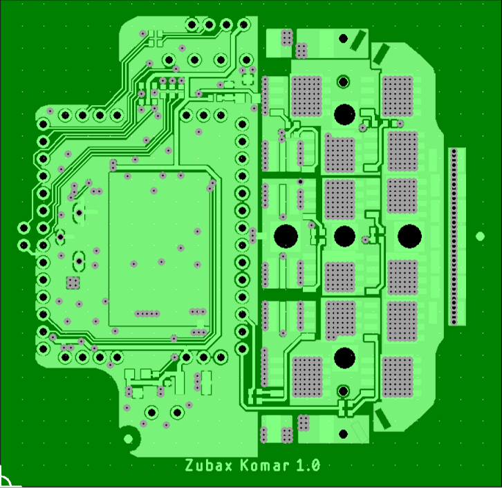
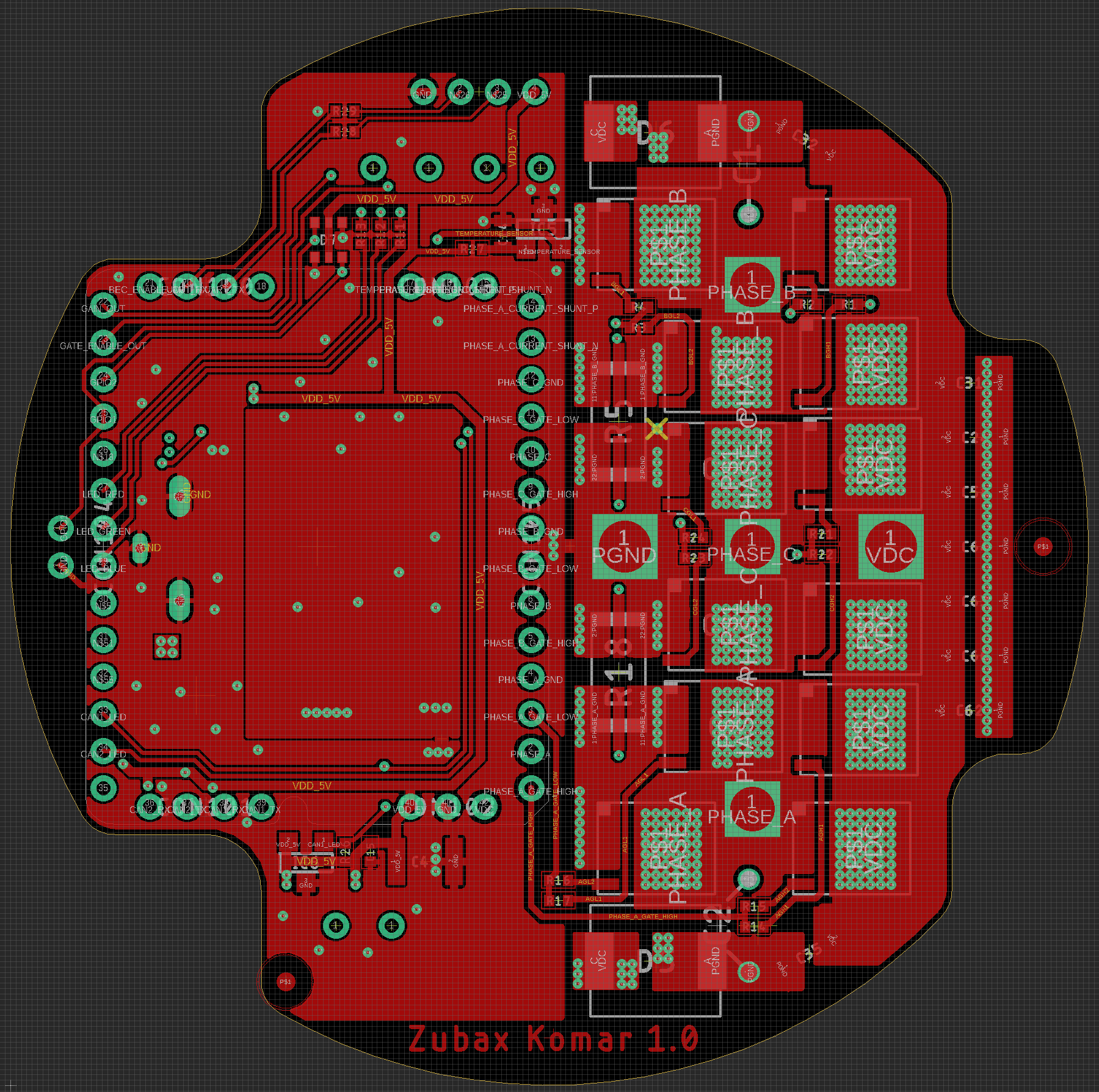
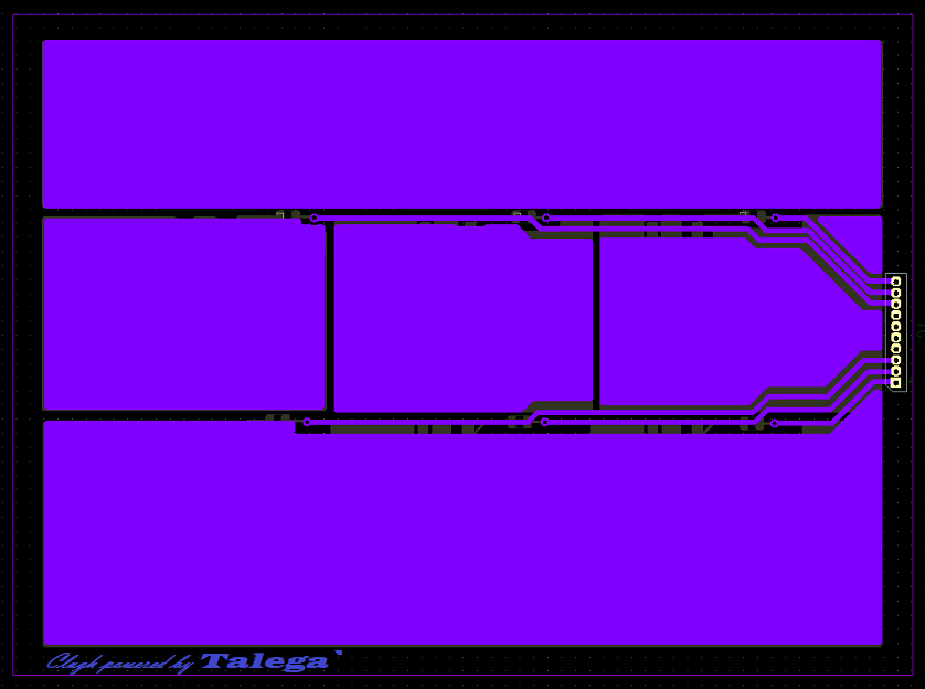
I have been working on my own PCB, but I am puzzled by the shunt connection on the two phases of the Komar. Am I correct that the two sensed phases must sink their current through the one un sensed phase pad to the B negative rail ?
That is not the correct description but it could be that misunderstood it. Please check section 2 of the Mitochondrik datasheet: https://files.zubax.com/products/com.zubax.telega/Zubax_Mitochondrik_LV_Datasheet.pdf. Notice that phases A and B contain the low-side sensing shunt resistors, while the low-side source of phase C is connected directly to the power ground.
Thank you Pavel,
You are correct I really should have looked at it that, The B- pads on the PCB is what is tied between the 3 phases. If you wanted even more current than the lowest shunt in this footprint can deliver is there a topology that will accurately feed multiple shunt measure into the mitochondrikLV 4 channels, or could you scale the 2 one from each parallel array in firmware?
I understood that you are constrained by the power dissipated at the shunt, is that correct? If you can’t use a larger (higher power) shunt nor a lower-resistance shunt but using more than one shunt is acceptable (this is an unusual combination of constraints), you can connect them in parallel, but there’s risk that the balancing current through the Kelvin sensing nets may affect the measurement.
Valenok is currently undergoing testing. Perhaps we could provide you a pre-production sample for evaluation; if this sounds interesting, please reach out to sales@zubax.com with a reference to this thread. Thanks!
Are you kidding that sounds absolutely incredible Pavel of course I am interested. I absolutely believe in the beauty of your device. The lowest shunts I’ve seen in the small footprint are 1milli. I don’t have to have an extremely small footprint. I have and electrical engineering degree and work at Wolfspeed in NC in the polish dept. I also plan to try Talega with a few SiCFET based bridges. ANY joint adventure, help beta testing, etc that I can provide I am all in. I think the mitochondrik is and absolutely wonderful device for high end industry and DIY projects. I have some motors winds that have really low resistances . Some less than a milli so Were looking at amperage levels around 13 Kw. I did some beta testing for APD PRO HV prototypes when I was at Daimler and am figure out how I can get around being able to run even more FETs in parallel. I think you have worked out this problem in the Valenok Im also looking at the Double cool side.FETS in a modular stack. I think you will like these better than the komars.
I have the ability to manufacture doube side PCB so I can put prototypes together. If you have a PCB template for the Velonok I can build the inverter. But I have some other motor and dirve ideas I think you’d really like .
Hi people
Sorry I’ve been away taking care of my father but I’m ready to get back into this discussion and work with your dynamite device. I’d like to ask has there been any progress with the valenok?
We are still validating the device in the lab. There has been some progress but right now the project is stalled until January due to upgrades to our test rig. We will be posting updates in the blog soon.
Good to hear . For now the Mitochondirk is good, Have you all done any work with GaNfet technology? I’m just now looking at it because I had been focused around the SiC.
Superjunction MOSFETs are gradually being replaced by both GaN and SiC. SiC appears to be the favorite for on-board chargers (OBCs). This trend will undoubtedly continue as engineers discover the newer devices and gain experience with them.