How I Learned to Stop Worrying and Love ESC Development

Explanatory Note: The text below contains some recommendations on how to develop a modern motor controller. It contains some recommendations to help the designer to get the job done relatively quickly without an infinite struggle with doubts and discussions at every possible aspect of the project. The text does not pretend to be academically rigorous, rather it is more about practical ways of solving particular problems. Quoting Captain Barbossa: “This is more a set of guidelines than actual rules.”

Many of us come to this idea at one moment of our lives – to the idea of developing a custom brushless motor controller. It may arise for different reasons: you’re building a high-end vehicle with very specific requirements or you just need a decent controller. There is a certain set of steps that are to be taken to achieve this goal, all of which involve knowledge from different fields. It may be difficult for a single person to be competent in all these fields so this text describes an easier way of completing this challenge successfully. It reduces the skills and competencies needed and also drastically reduces the development time.

Let’s list all the stages of custom ESC development (supposing that high-level requirements like power level, input voltage range etc. have already been put in place):

  1. Pick up the main components: power transistors, transistor driver, MCU, DC-DC converters, communication interface drivers and connectors etc.
  2. Carefully read all the datasheets to look for possible conflicts. (Just for reference, the datasheet for a modern transistor driver IC like DRV8350 from TI is a 100 pages long complex technical document).
  3. Create a schematic of the whole controller.
  4. Carefully think over the component arrangements taking into account things like possible electromagnetic issues, cooling and housing means, the ease of reach of the connectors, etc.
  5. Route the PCB; possibly, several times due to the errors made in the previous stages.
  6. Design a housing that is possible to manufacture using a selected technology (be it 3D printing or milling or whatever else).

All these steps, although they may not be that simple, take a finite amount of time. The last ones, however, may take forever and never be completed:

  1. Software development and debugging.
  2. A GUI will be most probably needed to configure the controller.

The problem with programming and debugging motor controllers (and power electronics in general) is that they require the developer to be familiar with motor control theory, linear algebra, common electrodynamics and, of course, embedded real-time programming. The means of debugging such systems is very limited too, as the process under control is very fast and involves high-energy transitions. It is impossible to just halt the MCU and inspect its internal state or to use other conventional debugging methods like printing out the variables to the serial output. Besides, if something goes wrong it often causes hardware damage so perfect repair and soldering skills would be helpful.

A few of words about reliability should be made. In many cases, a controller is intended to control a motor mounted on some kind of aerial vehicle. This imposes special reliability requirements because a controller failure may lead to catastrophic consequences, not least the aircraft will be most probably critically damaged. This means that the software must be very reliable which can only be achieved by following standards like MISRA and doing lots of testing.

Conspicuously, the development of a motor controller from scratch is a major effort and one in which results are not guaranteed. But there is a way to avoid most of the challenges involved: use an integrated module for PMSM/BLDC motor control to do all the heavy lifting. This is what Zubax Mitochondrik LV does. Of course, even with this help, the whole development process will be hardly a piece of cake but it does simplify it a lot. The main advantages are:

  • The only components that have to be selected are the power stage components, interface ICs and connectors. Generally, the hardest part is selecting the power transistors, proper capacitors and shunt resistors for the current measurements.
  • The schematic and PCB design are greatly simplified as all the complex circuitry is embedded into the module.
  • There is no need to mess with the DC-DC converter design as it is embedded into the module.
  • And most importantly; no programming needed. Mitochondrik LV runs Télega software which uses advanced and sophisticated algorithms to control the motor. Also, there is a standard GUI tool for Télega-based controllers already so no additional PC-software development is needed either.

Therefore, the application of Mitochondrik LV in motor controller development leaves the designer with many fewer problems to solve.

Below is an example of controller development using Mitochondrik LV using a Zubax Komar controller.

The initial requirements of the controller are:

  • Input voltage range: 20 – 50.4 V.
  • Continuous power output: 2 – 2.8 kW with a 12S battery where the range of possible battery voltages is 40 – 50.2 V.
  • Dimensional requirements: Circular and comparable in size to a compact 2 kW-rated motor like the T-motor MN5212.
2 Likes

Component selection

As this is a Mitochondrik-based device, the critical components to select are the power transistors, the current shunts, and the buffer capacitors.

Transistors

The search criteria for the transistors are:

  • VDS – not less than 80 V as there needs to be a safety margin above the maximum supply voltage of 50.4 V.
  • RDS(on) – the less the better as this directly impacts power loss and heat dissipation of the power stage.
  • Qgate – the less the better since the lower the Qgate, the faster it is possible to switch the transistor, resulting in less power loss and heat dissipation.
  • SMD package to keep things compact.

When speaking about the required current conducting capabilities of the power transistors, some clarifications need to be made. The current drawn from the battery (Idc) is not equal to the current that the transistors need to handle, known as the phase current (Iphase). In general, the phase current is higher than the battery current.

The relation between the DC power, AC power, and the mechanical power delivered to the shaft is a little involved. This topic is covered in detail in the chapter on motor control fundamentals in the Telega Reference Manual. The synopsis is:

P_\text{dc} = u_\text{dc} \, i_\text{dc} \approx \frac{3}{2} \left( u_q \, i_q + u_d \, i_d \right) \approx \omega \, \tau = P_\text{mechanical}

A helper spreadsheet is linked there as well, which allows one to determine the AC and DC power components based on the motor parameters and the required load torque and velocity. An example estimation is given below for some application:

In our case, we obtain I_\text{phase_max} \approx 65 A. This is an amplitude value; the RMS is therefore I_\text{rms_max} = \frac{I_\text{phase}}{\sqrt{2}} \approx 46 A.

Important: Iphase_max is not the absolute maximum phase current that the device can handle. Rather, it is the maximum continuous phase current and is limited by the thermal budget of the device. The absolute maximum phase current (Iphase_peak) is determined by the overcurrent protection trigger level (more on that below).

Now it is possible to select a power transistor. After some research BSC040N08 from Infineon Technologies was selected:

Assuming that the maximum switching frequency for Mitochondrik in this application is 47 kHz (it is configurable from about 10 kHz up to approx. 120 kHz, more on this in the Telega Reference Manual), it is possible to calculate the average “on-time” for the transistor:

\begin{aligned} T_\text{on} &= \frac{1}{2 \cdot F_\text{sw}}\\ T_\text{on} &= \frac{1}{2 \cdot 47000}\approx 10 \mu s \end{aligned}

The image above shows that the selected transistor fits the application at the end of its tether. But one should keep in mind that this is valid at 25℃ transistor case temperature. As the temperature rises, things get considerably worse. And the temperature will definitely rise noticeably (more on that later).

The solution is to use two transistors in parallel per half-bridge side. Of course, it is also possible to find some bigger transistor, but due to the geometric limitations, 12 smaller transistors are preferable to 6 bigger ones.

Another important thing to check is whether the Mitochondrik can switch the selected transistors fast enough. From the Mitochondrik datasheet, the average gate drive current (Idrive_avg) is 25 mA. The gate charge of a single transistor is Q_g = 54\ nC. The transistors can be used if the following holds:

\text{Gate Drive RMS Current} < I_\text{drive_avg}

and:

\text{Gate Drive RMS Current} = Q_g \cdot n \cdot F_{switching}

where:

  • n is the number of switching transistors.

In Télega, two thirds of all transistors are switched concurrently. In a typical vector control drive all transistors are switching continuously but Télega leverages sophisticated modulation strategies to reduce the switching losses. For Komar, this means 8 transistors.

\text{Gate Drive RMS Current} = 54 \cdot 10^{-9} \cdot 8 \cdot 47000 \approx \text{20.3 mA}

This is less than the Mitochondrik’s capabilities, so the configuration is admissible.

Current shunts

There are numerous ways to measure the current flowing in the conductor: current shunts, hall effect sensors, even digital compasses as TI suggests. Mitochondrik uses the simplest and the most cost-effective approach – it measures the phase current using low-side resistive current shunts. Selecting the current shunt is always a trade-off between the heat dissipated in the shunt (i.e. power loss) and the dynamic range of the measurement. For a Mitochondrik-based controller there are two criteria for selecting shunts: 1) resistance; and 2) power rating.

The optimal resistance of the shunt is derived from the voltage measurement dynamic range when the current reaches its maximum value. For Mitochondrik-based controllers, this is 0.135 V. The maximum phase current (Iphase_max) was determined beforehand to be 65 A. This enables us to derive the optimal resistance:

R = \frac{0.135}{65}

The closest standard value is 2\ \text{m}\Omega.

Mitochondrik-based controllers use current shunts on two of the three phases (A and B only). According to this, the maximum power dissipation in one current shunt can be determined as:

\begin{aligned} P_\text{max} &= \frac{R\ I_\text{rms_max}^2}{2}\\ I_\text{rms_max} &= \frac{I_\text{phase_max}}{\sqrt{2}}\\ P_\text{max} &= \frac{0.002\ (\frac{65}{\sqrt{2}})^2}{2} = 2.1125\text{ W} \end{aligned}

For the described controller, the shunt CRE2512-FZ-R002E-3 from Bourns Inc. is selected:

Capacitors

A few words about the bulk capacitance: why is it needed, in general?

The main purpose of a motor controller is to convert the electric energy stored in the battery into the mechanical energy of the spinning motor. In an ideal world, there are no parasitic effects in the electrical circuits. The motor controller would be able to draw the electrical energy without obstruction and could drive the motor at any frequency using PWM with zero rise time; all without causing any issues. The overall schematic would look like the picture below:

In real life however, parasitic properties are all over the place. With some simplification, a more realistic version of the system might look like:

While the parasitic resistance only causes the wires to heat up (and sink energy into the environment), the parasitic inductance is a different story. It limits the rate of temporal change of the supply current (\frac{dI}{dt}). The system responds to current variation with a change in voltage. The voltage ripple on the motor controller side of the system leads to several undesirable effects: heat loss, noise, distortion of measurements, and electromagnetic interference.

There is second potential pitfall that should not be forgotten. The energy conversion that takes place in the motor controller is in fact bidirectional. The spinning rotor (especially with some kind of mechanical load attached) has some kinetic energy. In the case of braking, this energy has to be removed from the rotor and redirected elsewhere. In most systems, it would go back to the battery and recharge it a bit but due to the parasitic inductance and resistance between the motor controller and the battery, this energy may induce a voltage spike on the motor controller side with the potential of causing severe adverse effects on the stability of the motor control loops or the hardware itself. This is the second reason to have local energy storage in the form of bulk capacitance within the motor controller itself.

The size of this local energy storage depends on many factors (battery wires’ length, their thickness, the way the wires are routed, etc.), so adequate design and system-level testing is always required. But there is a practical rule of thumb: use at least 20 uF of DC bulk capacitance per 1 A of DC bus current.

The capacitor bank usually consists of capacitors of two types: electrolytic capacitors with high capacitance and high ESR along with ceramic capacitors with much lower capacitance but very low ESR. Electrolytic capacitors help reduce the low-frequency ripple while ceramic ones are effective against high-frequency noise. In the absence of adequate system models, the required amount of ceramic capacitors may be determined empirically, in which case extra PCB footprints may be helpful.

One additional recommendation about the capacitor selection is that it may be beneficial to use several smaller capacitors and connect them in parallel rather than one massive capacitor. It may not only reduce the overall size of the motor controller but also reduce the effective ESR of the capacitor bank making it more effective.

These are the parameters that should be taken into consideration when selecting the capacitors:

  • Voltage rating – shall be no less than Vin_max.
  • Capacitance – may only be limited by the cost, size, and weight constraints.
  • ESR – in general, the less the better.
  • Lifetime expectancy – electrolytic capacitors tend to degrade considerably over time and this process is accelerated with the high temperatures (which is usually an issue in any motor controller).

According to the parameters above, two B41888C8227M capacitors (220µF 63V Aluminum Electrolytic Capacitor, 7000 Hrs @ 105°C) from TDK are selected.

The capacitor bank was complemented with 9 (3 per phase) 4.7 uF ceramic caps. This setup yields a total of ~460 uF, a value lower than the recommended capacity from the rule of thumb above (but then again there is a reason why it is called a “rule of thumb” and not a “rule of law”).

Schematic development

The schematic development is hardly interesting at all as it is basically a copy-paste straight from the datasheet. It is shown below:

Overcurrent protection

One matter that probably does need an explanation is overcurrent protection. Mitochondrik constantly monitors the voltage drop across the power transistors. It compares the voltage drop against the voltage on its oc_adj pin, which is set by an external resistor using the following formula:

I_\text{trip} = \frac{3.3\ R_\text{oc_adj}\ 10^{-3}}{ (10 + R_\text{oc_adj}10^{-3})\ R_\text{side}}

where:

  • R_\text{oc_adj} is the value of the protection trip level setting resistor [Ohm].
  • R_\text{side} is the half-bridge side resistance [Ohm]. For example, in Komar, each half-bridge side is composed of two parallel transistors, each has R_\text{DS(on)} = 4.3\ \text{m}\Omega, which yields:
R_\text{side} = \frac{4.3}{2} = 2.15\ \text{m}\Omega

In the case of Komar, I_\text{trip} is set to 130 A, a level which is 2 times higher than the maximum continuous phase current but is within the safe operating range of the selected transistors.

From the equation above we obtain:

R_\text{oc_adj} = 1K

Last, but not least the RDS(on) of individual transistors changes with temperature considerably, and does the Itrip. At 85℃, Itrip will be approximately 1.5 times lower than it would be at normal operating temperature of 25℃; i.e. at around 90 A.

Gate resistors

Another sore subject is gate resistors, particularly their value and number. It is recommended to have series resistors for power transistor gates. In the case of parallel transistors, a separate gate resistor for each transistor should be used.

The main and only purpose of having the gate resistors is to eliminate ringing in the gate circuits. The ringing appears because PCB traces have stray inductance and transistor gates have stray capacitance and all this acts as an oscillating circuit. The lower the signal rise time is, the worse the oscillation gets. A gate resistor increases the rise time, thus reducing the oscillation. Steeper fronts, on the other hand, generally reduce the switching losses. The required gate resistance should be obtained by modeling the PCB parameters. Alternatively, trivial empirical methods could also be employed.

PCB and construction

At this point, it is crucial to have some physical representation of the final result: at least the overall shape, dimensions and connector placement should be known by this time.

Two main questions to address when designing power electronics and supercomputers are:

  1. How does one deliver all the necessary power to the device without substantive power losses?
  2. How does one cool everything that heats up?

Both of these questions have a direct relationship to the power stage PCB design. Routing high currents through the PCB is generally not the best idea as the copper foil thickness is typically in the range of 0.035 – 0.105 mm (n.b. thicker foil imposes more restrictions on the PCB design due to the limitations of the PCB manufacturing process). There is an upper limit to the amount of current that can be routed conventionally through a regular FR4 PCB; as an oversimplified rule of thumb, this limit is between 50 – 100 A. Anything above this limit would require special measures (e.g. busbars, PCB trace reinforcement, etc.).

Fortunately, Komar’s maximum phase current allows it to be routed on a regular PCB, although it still requires the power stage to be properly designed. The key element here is the component arrangement. The designer should minimize the path of high current through the PCB (if high current barely touches the PCB copper, it can’t influence the PCB too much). All the connections that carry high currents should be made with polygons to ensure that the electrical resistance is minimized. Polygons also serve as heat distributors, removing heat from transistors (and other heating components) and spreading across the PCB. This in turn increases the effective contact area between the PCB and the heatsink. It should be noted that the transistor’s R_\text{DS(on)} is a temperature-dependent parameter, which is why it is important to ensure that the thermal load is distributed equally across the transistors. This is the second role of big polygons: they should couple all the transistors thermally together.

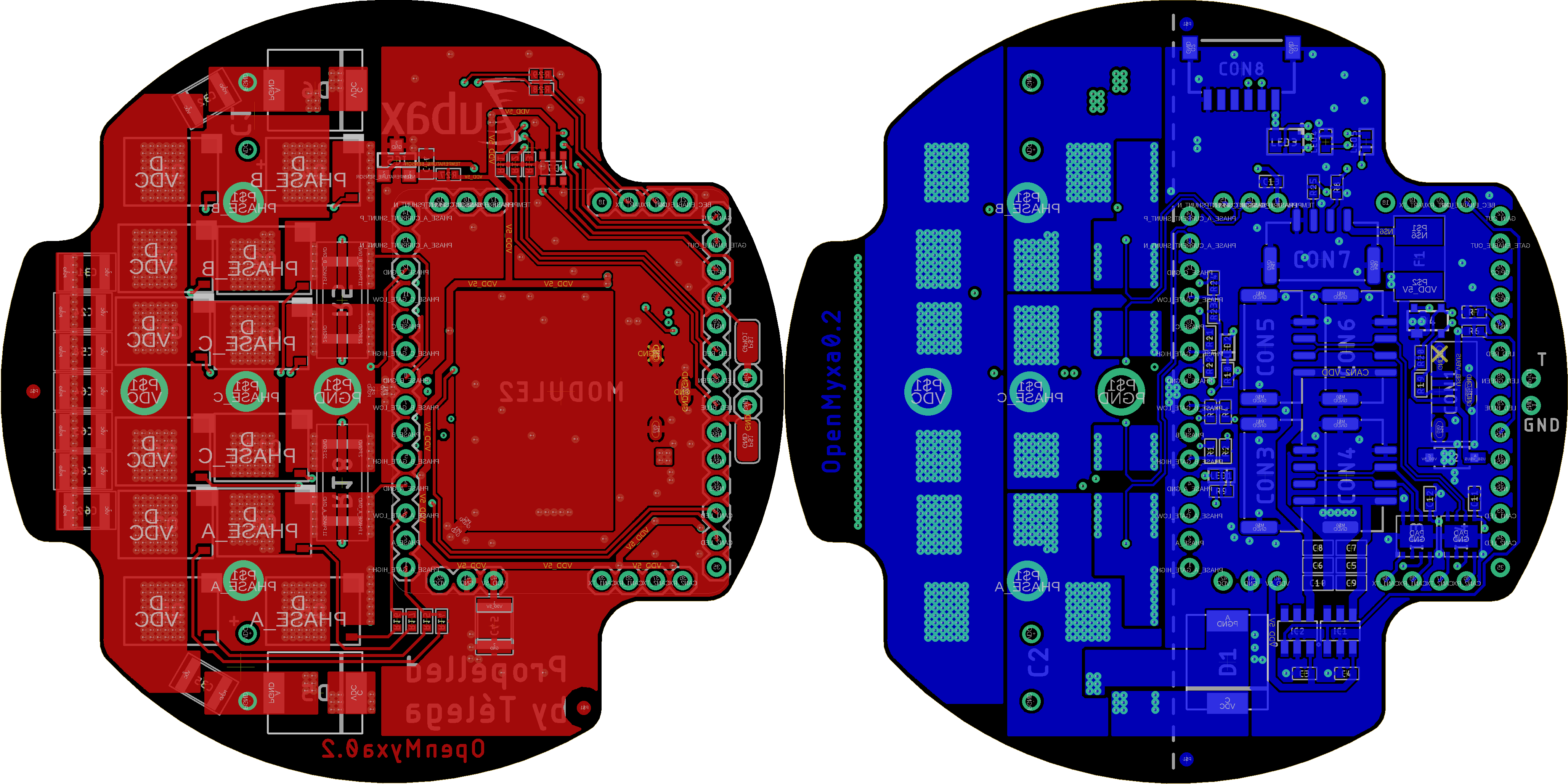
The second important design challenge, after providing a good path for the power input, is cooling. There is more than one way to cool electronic components but the simplest and most cost-effective one is air-cooling. Usually, some kind of heatsink that dissipates heat into the environment is suggested. First, though, the heat needs to be transferred to the heatsink. The designer should minimize the thermal resistance between the transistors’ junctions and the heatsink.

As an example, Komar uses power transistors in the PowerTDFN-8 package. Its thermal resistance is described in the following table:

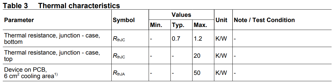
It should be obvious that the heat from the transistors is transferred much more efficiently to the PCB through the bottom of the transistor housing than through the top. When heat is transferred to the top side of the PCB it should be transferred onward to the bottom side and then to the heatsink. Multiple via holes help the heat to get to the bottom side of the PCB. The exact thermal impedance of a via depends on the PCB manufacturing process, the via’s diameter, and the PCB’s thickness. Here is a good article on the topic:

Long story short, many smaller vias perform considerably better than fewer bigger ones because it is the total surface area of metal connecting the two sides of the PCB that matters. Consequently, it is highly recommended to fit as many vias as possible on the transistors footprints and position them for best thermal performance. The only practical way of transferring the heat onward to the heatsink is just to press the heatsink to the PCB mechanically. Of course, this requires that there are no components on the bottom side of the PCB (or at least, there are no components directly under the transistors).

Important note: In most cases, the heatsink is not directly attached to the PCB (or other objects that needs cooling) but through some kind of thermal pad. In the case of Komar, a thermal pad is needed because there are many different signals and polygons on the bottom side of the PCB and as the soldering mask is not a proper insulation something may short. The designer should keep in mind that thermal pads may have drastically different thermal resistance so care is needed in selecting one. The second important consideration is that thermal pads are specified under pretty strict conditions, the most important of which is pressure. You may pick the best thermal pad available to a mortal man but if you don’t provide it with the specified pressure, it won’t perform any good. Of course, this matter does not relate to the PCB routing directly but it still has to be mentioned.

The worst-case power losses in the power stage are calculated next. First, the maximum power loss for one individual switch are calculated, where by “switch” we refer to a group of transistors forming an inverter node (in our case, that would be two transistors in parallel). The coefficients next to the loss components account for the fact that normally, only 4 of the 6 switches are switching (of the other two, one is constantly closed and one is constantly conducting DC) and at any given moment only 3 switches out of 6 are conducting:

\begin{aligned} P_\text{loss} &= \frac{1}{2} P_\text{loss_ohmic} + \frac{2}{3} P_\text{loss_switching}\\ P_\text{loss_ohmic} &= I_\text{rms}^2 \cdot R_\text{DS(on)}\\ P_\text{loss_switching} &= {V_\text{dc} \cdot I_\text{rms} (T_\text{rise}+T_\text{fall}) \cdot F_\text{switch}} \end{aligned}

where:

  • F_\text{switch} = 47 000\text{ Hz}
  • V_\text{dc} = 50.2\text{ V}
  • I_\text{rms} = \frac{65\text{ A}}{\sqrt{2}} (the peak phase current flowing through one switch is 65 A)
  • T_\text{rise} = 50 \times 10^{-9}\text{ s}
  • T_\text{fall} = 50 \times 10^{-9}\text{ s}
  • R_\text{DS(on)} is that of the switch rather than an individual transistor (twice lower in our case)

Now the total power stage losses can be calculated using the power loss in a single switch along with the losses in the current shunts that were found earlier:

P_\text{loss_total}= 6 P_\text{loss} + 2 P_\text{shunt_loss}

This is an approximation because many system parameters are temperature-dependent and are, therefore, constantly changing. We are also not considering losses through the flyback diodes, as they are typically quite low in a well-designed modern inverter with tight dead times (n.b.: Mitochondrik controls the dead time automatically in hardware).

The last thing needed for the thermal simulation is the convection rate. This is a tricky one and usually has to be picked from existing convection tables. For forced-air convection, the rate may be 300\ \frac{W}{m^2 K} depending on the intensity of the airflow around the heat sink.

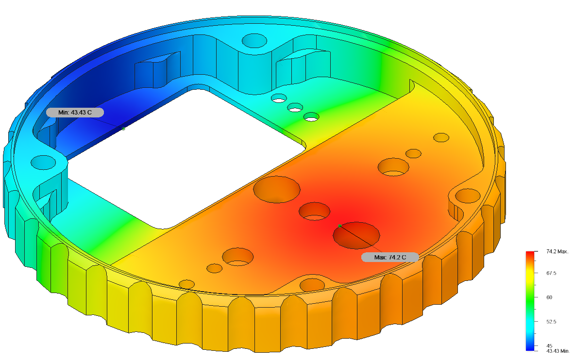
For the sake of simplicity, the simulation does not involve the actual PCB with transistors. It is just about the ability of the heatsink to dissipate the rejected energy under the specified convection rate. It is seen that the temperature gradient is moderate (especially considering the shape of the object) and the maximum temperature is below 80°C. One should keep in mind that the actual temperature of the semiconductor crystals will be higher than the temperature of the heatsink due to the non-zero thermal impedance between the crystals and the heatsink (n.b. this difference may exceed 50°C).

All the reasoning above indicates that with a device like Komar, it is possible to sustain continuous operation at the power levels as high as 2.5 kW. Further confirmation would require prototype manufacturing and testing on actual hardware. These tests have been conducted and the results were found to be sufficiently similar to the model predictions.

All the hardware source files can be found in the GitHub repository.